VITUS
H20LE
30 mm² collimated to 20 mm² X-ray Silicon Drift Detector for Low-Energy XRF – EDX – TXRF – Applications
Unique Features
- Large area low-energy module
- Ultra thin polymer window
- Sensitive down to Boron Kα at 185 eV
KEY PARAMETERS
(Guaranteed Values)
| CUBE CLASS |
|
|---|---|
| First amplification stage | ASIC |
| FWHM Mn Kα (5.9 keV) | ≤ 129 eV |
| FWHM C Kα (277 eV) | ≤ 70 eV |
| Peak to background | > 10,000 |
| Peak to tail | > 2,000 |
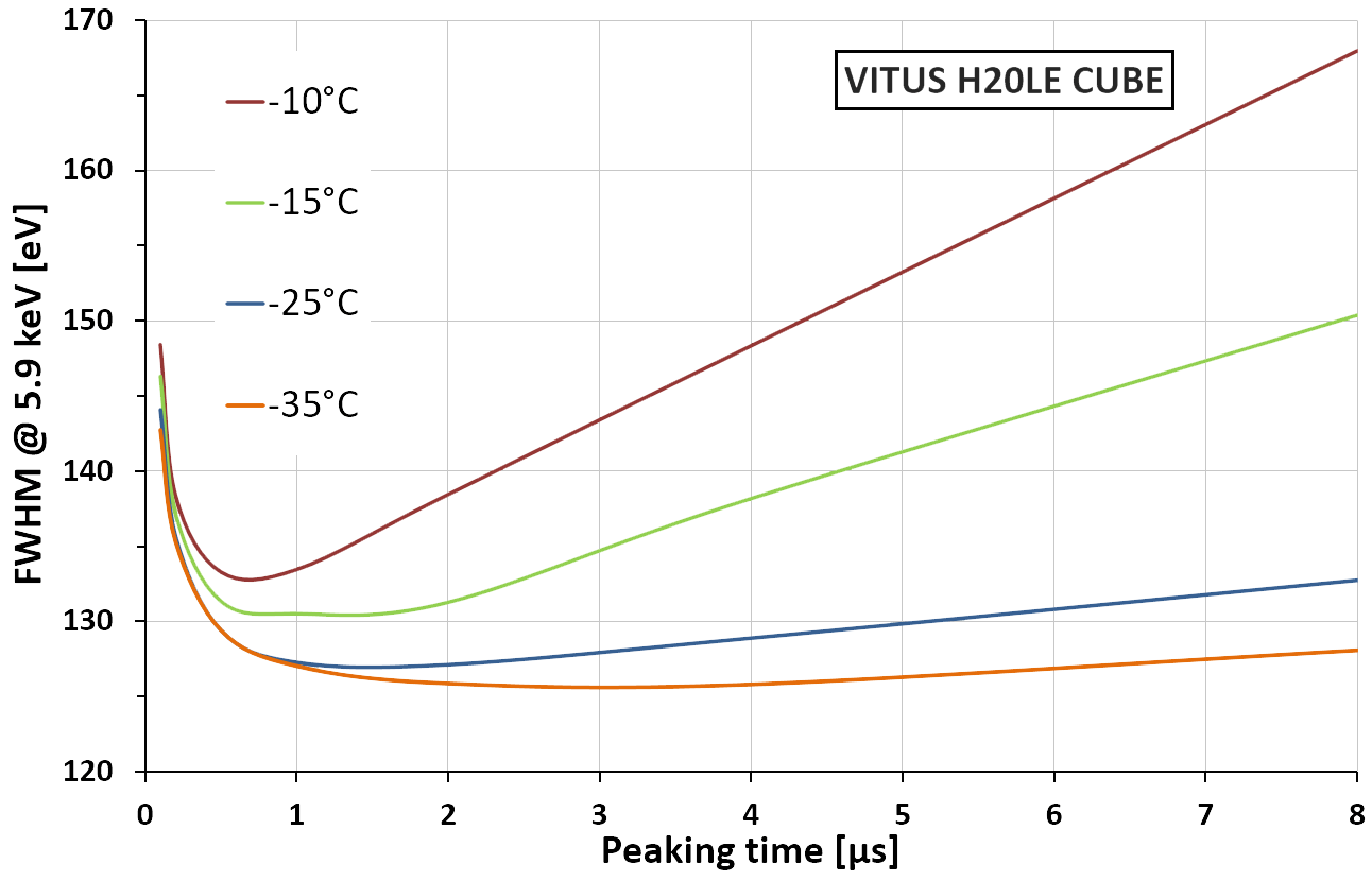
| Optimal peaking time at max. cooling | 1 µs |
| Absorption depth Si | 450 µm |
| Peak shift stability up to 100 kcps | < 1 eV |
| Max. input countrate | 2,000 kcps |
| Windows | AP3.3 polymer |
| Cooling performance at +30°C heat sink temperature |
∆T > 65 K |
| On-chip collimator | Pd |
| Ordering codes | V000-C7T0-H020-PD3E 129 |
Spectrum
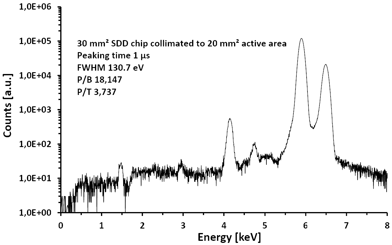
Figure 1: The spectrum has been acquired in KETEKs standard end qualification test stand with an Fe-55 source using an XIA Mercury signal processing unit. The input count rate has been 10 kcps at a peaking time of 1 µs. The spectrum shows a very good energy resolution for Mn-Kα and an excellent peak-to-background ratio.
OPERATION REQUIREMENTS
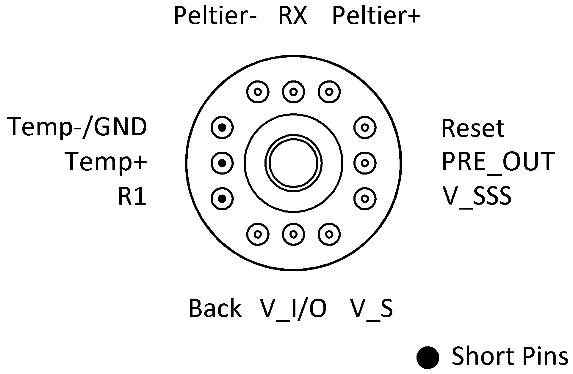
SDD Voltages and Currents
| Ring1 (R1) | -20 V ± 5 V | 10 µA typ. |
|---|---|---|
| RingX (RX) | -130 V ± 20 V | 10 µA typ. |
| Back | -60 V ± 5 V | < 1 nA |
| Peltier Element | 4 V | 1000 mA max. |
General parameters
| Temperature Monitor | NTC thermistor | 10 kΩ @ 25 °C |
|---|---|---|
| Output signal | ramped reset type | – |
CUBE based SDDs
| VI/O | 3.3 V ± 0.1 V | < 1 mA |
|---|---|---|
| Vs | 2 V ± 0.1 V | < 1 mA |
| Vsss | -5 V ± 0.1 V | < 1 mA |
| Output gain | 1.6 mV/keV ± 20 % | – |
