SDD Operation
For (optimal) operation, SDDs require the application of several voltages and integration with a charge sensitive amplifier and other pulse forming electronics (either analog or digital). Typically, a high voltage DC power supply feeds the drift ring voltages; a high current, linearly regulated, low voltage power supply feeds the Peltier element; and a bipolar, linearly regulated power supply feeds the charge sensitive amplifier and pulse forming electronics.
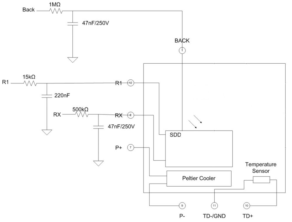
The drift ring voltages can be generated from a filtered high voltage rail, by using several voltage dividers. Each detector may have individual ring currents. Thus potentiometers should be used for voltage adjustments as the voltage drop at the voltage dividers depends on the ring currents.
The Peltier power supply should be regulated with a PI/PID loop to keep the operating temperature of the SDD chip stable. Therefore it is necessary to read out the temperature sensor of the SDD.
Wiring
The SDD should be placed as close as possible to the preamplifier. It is recommended to shield at least the preamplifier connections. It is strongly recommended using a single point ground. Please note that also the housing of the SDD should be connected to ground.
Mechanical Connection
WARNING: Do not operate the detector without proper heat sink connection. Overheating of the detector will destroy the module.
It is strongly recommended to install the detector connected to a proper heat sink. Dimensioning the heat sink is dependent on ambient temperature, air ventilation, operating temperature of the SDD, surface area and its condition. The guaranteed operating temperature is always related to the heat sink temperature. Therefore the minimum operating temperature can vary and is directly dependent on the quality of the heat sink interconnection.
Read-out Circuit for Temperature Sensor
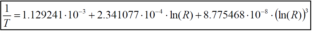
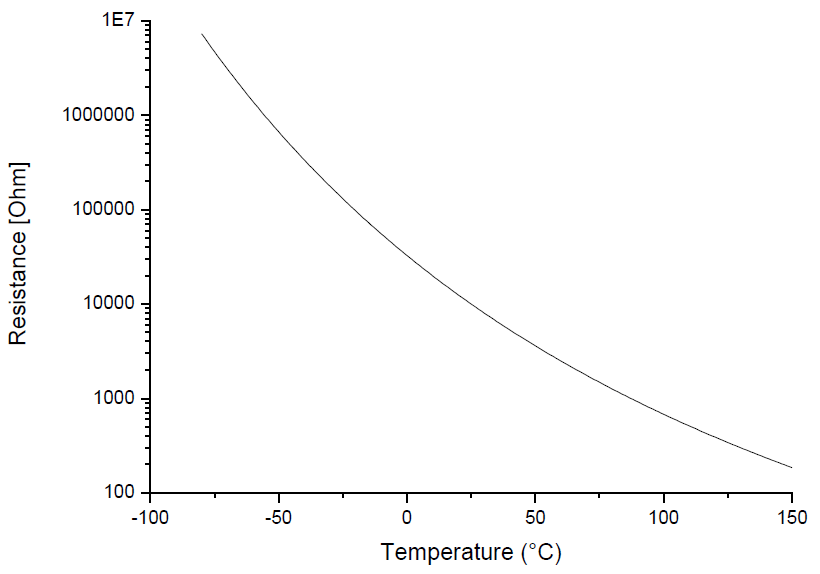
In case of the thermistor the temperature function is given by the following equation:
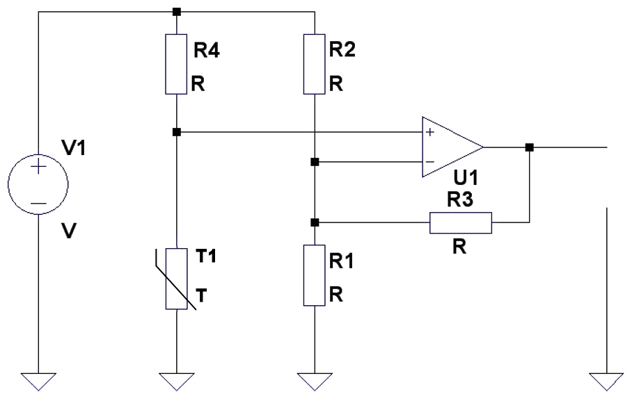
R4 limits the maximum current through the temperature sensor and should be set as follows:
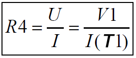
For example: The voltage V1 is +5 V and the current I(T1) should be 1 μA. This leads to R4=5 MΩ. R1 and R2 form a voltage divider representing the offset voltage. They can be used to set the circuit’s signal swing, given the operational demands on the SDD.
e.g. if an ADC is used to digitize the voltage, tuning R1 and R2 would ensure the desired temperature range corresponds to voltage values in the ADC’s range.
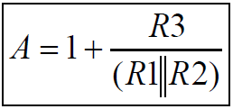
R1, R2 and R3 determine the gain of the circuit. The gain can be calculated as follows:
Operating Voltages
Several voltages are needed for operating the detector (exact values are given in each detector data sheet), for example:
- Ring 1 = approx. -20 V
- Ring X = approx. -130 V
- Back = approx. -65 V
The detector voltages should be filtered using the following combinations of resistors and capacitors providing low pass filters:
- Ring 1: RR1 = 15 kΩ, CR1 = 220 nF
- Ring X: RRX = 500 kΩ, CRX = 47 nF/250 V
- Back: RBack = 1 MΩ, CBack = 47 nF/250 V
Before switching on the system, the output-signal of the preamplifier and the shaped signal should be connected to an oscilloscope. The preamplifier operating voltage must be switched on first.
The detector voltages should be switched on in the following order:
R1 – RX – Back
The voltages to be applied must be set according to the detector datasheet. Typical currents flowing are several μA through Ring 1 and Ring X (voltage divider) and approx. 1 nA for the back contact if the back voltage is applied. R1 and RX currents should be equal!
After switching on the detector voltages the signal of the preamplifier should show a ramp. The ramp period depends on the chip temperature. At -35 °C the ramp period should be in the range of several microseconds.