Silicon Drift Detectors
KETEK’s Silicon Drift Detectors (SDD) are the state-of-the-art X-ray sensors for the energy range between 0.05 keV and 30 keV.
They are globally used in manifold applications in electron microscopes, XRF benchtop and XRF handheld spectrometers as well as in material sorting systems for mining and recycling. Due to their wide operating temperature range, their excellent energy resolution, and high reliability they are particularly suited for industrial applications.

VITUS H50 CH
65 mm² collimated to 47 mm² X-ray Silicon Drift Detector for XRF – EDX – TXRF Applications
Unique Features
- High performance module
- Largest area in ultra compact TO8 housing
- New KETEK CSA improves the energy resolution at all peaking times
- ∆T from 95 K to 130 K depending on heat sink temperature
- Power consumption as low as 250 mW possible at 20 °C heat sink and -35 °C chip temperature
- Superior radiation hardness up to a total dose of 5×10¹² incoming low energy photons
- Both Graphene window types available
- Operation under vacuum and under helium atmosphere possible
Available in
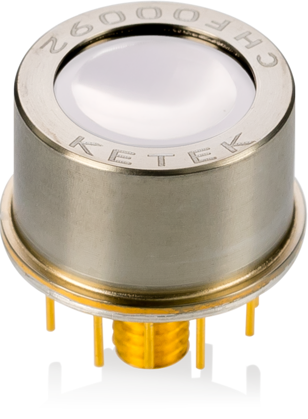
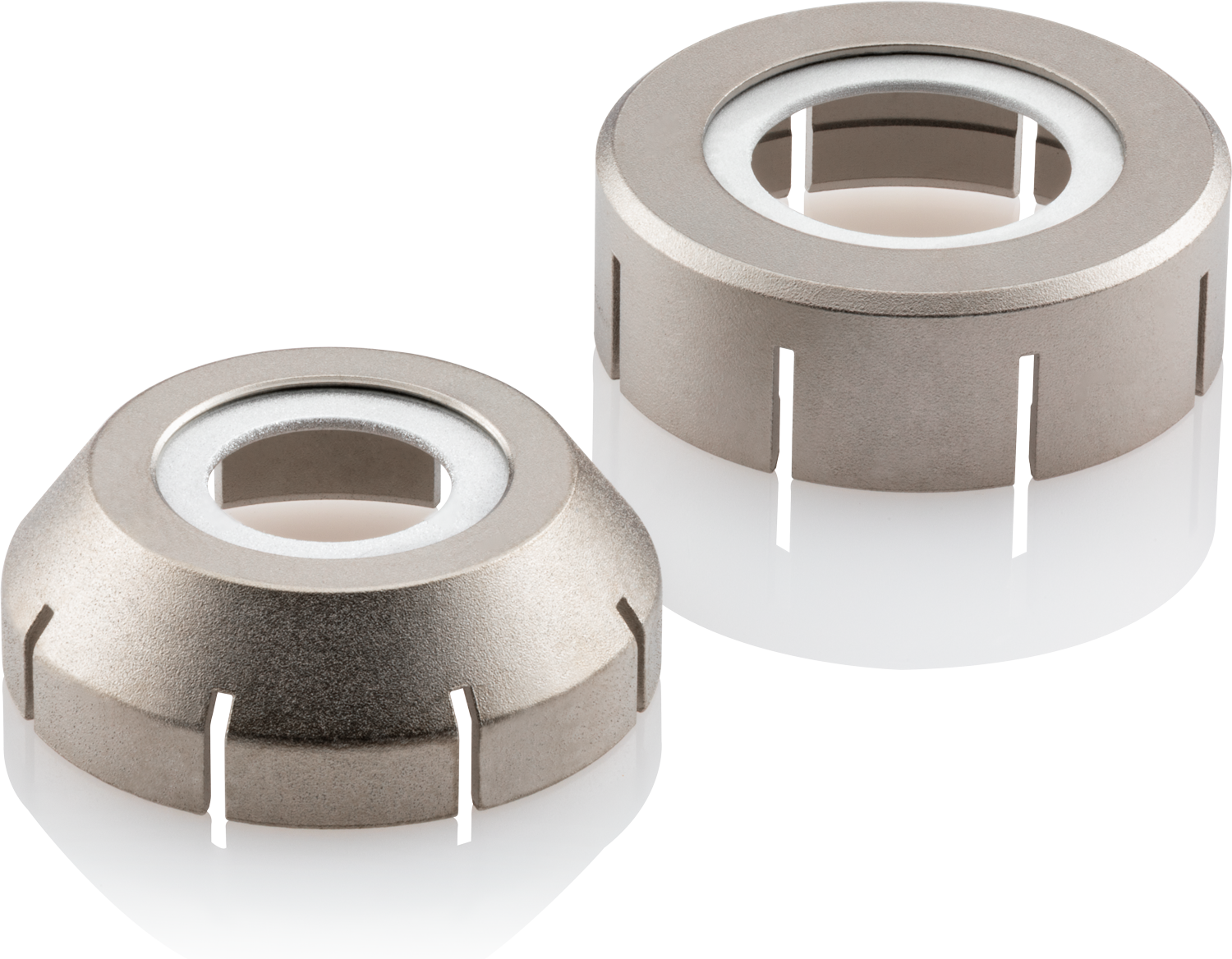
Vacuum encapsulated VITUS H50 in TO8 housing with CH window
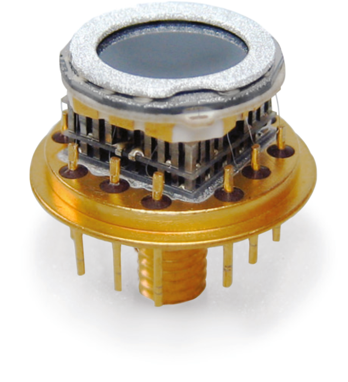
VITUS H50 with on-chip multilayer collimator before vacuum encapsulation
Available Options
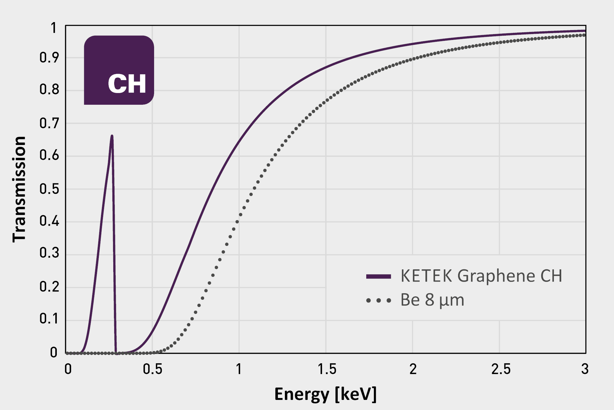
CH Window
1 µm Carbon, replacing 8 µm or 12.5 µm Beryllium
Vacuum encapsulated for many years of stable operation
No window fluorescence lines (pure Carbon)
Specifications
| First amplification stage | KETEK CSA |
| Energy resolution (@ Mn Kα, -35 °C chip temperature and 1 µs peaking time) | ≤ 129 eV |
| Peak to background | > 15,000 |
| Peak to tail | > 2,000 |
| Optimal peaking time at max. cooling | 1 µs |
| Absorption depth | 450 µm Si |
| Peak shift stability up to 100 kcps | < 1 eV |
| Max. input countrate | 4,000 kcps |
| Window | 1 µm Carbon |
| Cooling performance at +20 °C heat sink temperature |
∆T > 95 K |
| On-chip collimator | multilayer |
Spectrum
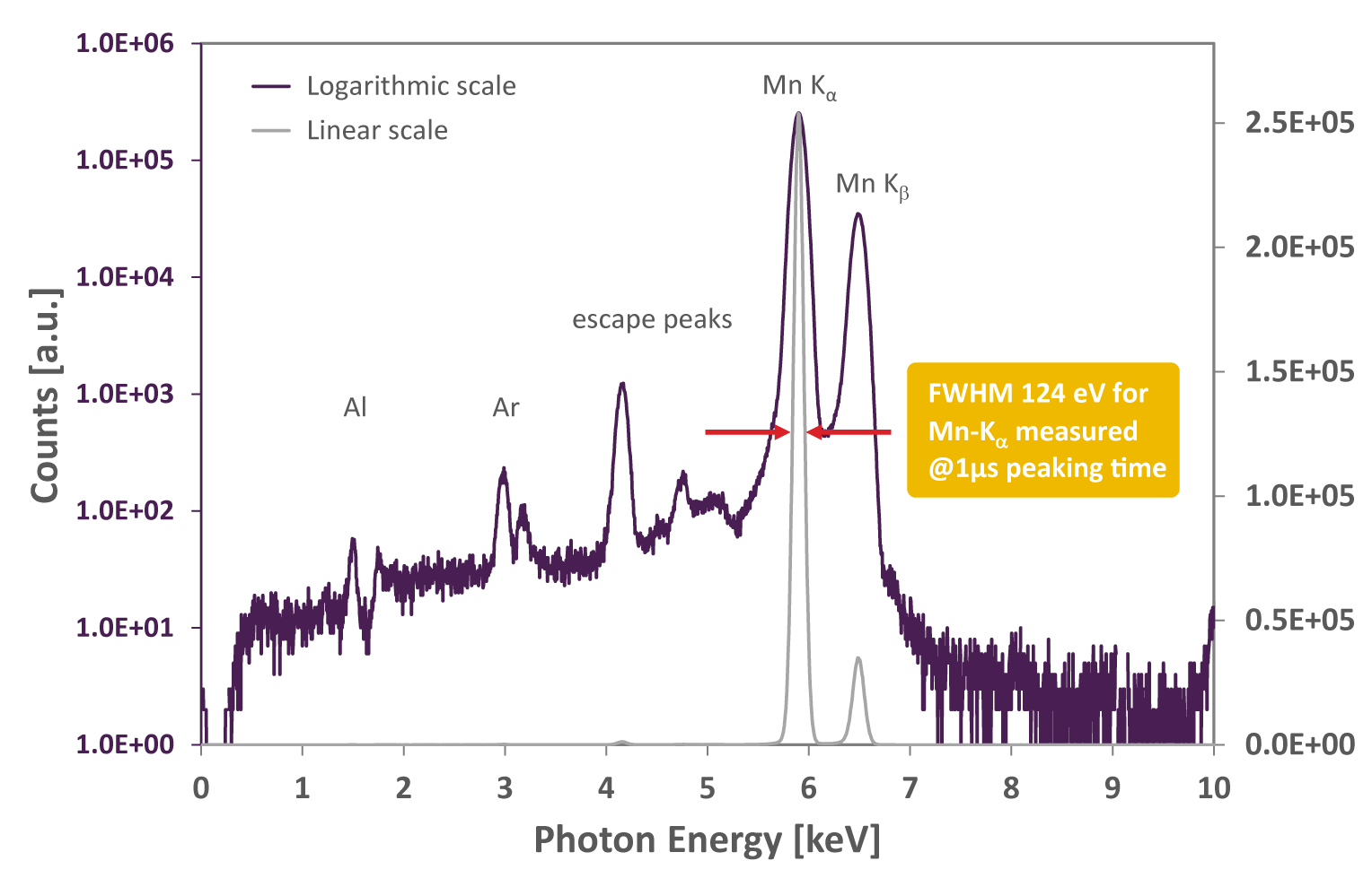
The spectrum has been acquired in KETEK’s standard end qualification test stand with an Fe-55 source. The input count rate has been 50 kcps at a peaking time of 1 μs. The spectrum shows an excellent energy resolution for Mn Kα and peak-to-background ratio.
Energy Resolution
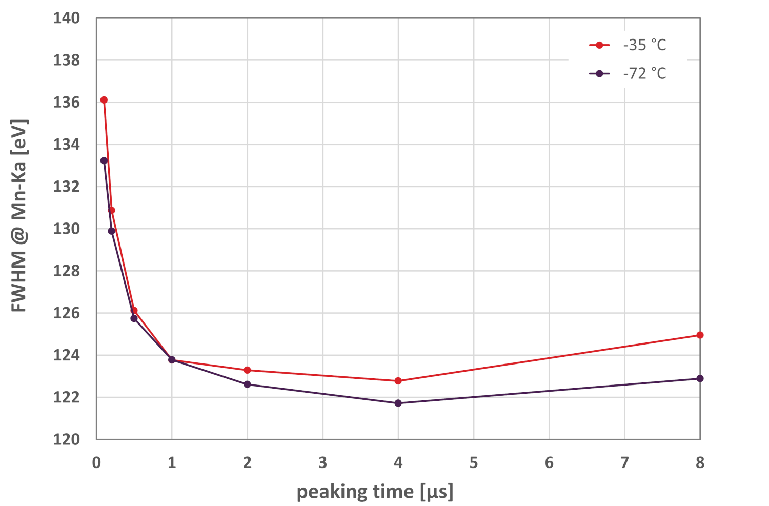
Energy resolution (Mn Kα) values for peaking times from 0.1 μs through 8 μs showing good FWHM values even for higher operating temperatures. Depending on the application the best performance can be achieved by an appropriate selection of peaking time and set operating temperature.
Cooling Performance
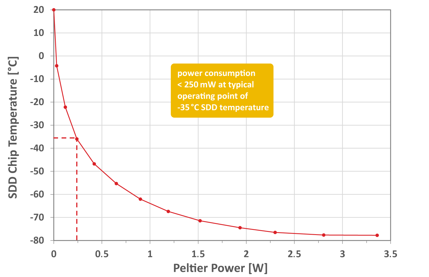
NEW SDD COOLING TECHNOLOGY
- -60 °C SDD chip temperature achievable even at +65 °C heat sink temperature
- Drastically increased efficiency of the thermoelectric cooling (e.g. 250 mW at -35 °C sensor temperature)
- Ultra stable vacuum integrity for typically more than 10 years of operation
Operation Requirements
SDD Voltages and Currents
| Ring1 (R1) | -20 V ± 10 V | 10 µA typ. |
| RingX (RX) | -130 V ± 30 V | 10 µA typ. |
| Back | -80 V ± 20 V | < 1 nA |
| Peltier Element | 5,5 V | 600 mA max. |
General Parameters
| Temperature Monitor | NTC thermistor | 10 kΩ @ 25 °C |
| Output signal | ramped reset type | – |
CSA Parameter
| VI/O | 3.3 V ± 0.1 V | < 1 mA |
| Vs | 2 V ± 0.1 V | < 1 mA |
| Vsss | -5 V ± 0.1 V | < 1 mA |
| Output gain | 1.6 mV/keV ± 20 % | – |
Pin Assignment

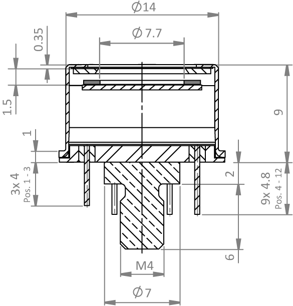
Geometry
Overview VITUS SDD Series
KETEK offers a broad range of high performance Silicon Drift Detectors (SDD) for energy dispersive X-ray spectroscopy. From mature off-the-shelf systems to innovative customized solutions, KETEK provides the right X-ray sensor for your needs across the spectrum of scientific and industrial applications. The VITUS SDD series combined with KETEK’s complete electronics including the pulse processing is a fast and efficient acquisition solution of highest quality.


Related Products
Available Signal Processing Electronics & Accessories