VIAMP
The VIAMP preamplifier modules are specially designed printed circuit boards for operation with KETEK’s VITUS Silicon Drift Detectors (SDD). The assembly comprises an ultra-low noise, ramped reset type electronic preamplifier of positive polarity with onboard settings and filtering for all necessary SDD bias voltages.
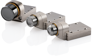
Depending on the size and application of the SDD module, three standard Aluminum housing options are available for the electronic boards, which provide appropriate protection and serve as a sufficient heat sink.

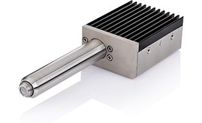
VIAMP-KL 3.0
VIAMP-KL 3.0 with a housing for large active area VITUS modules H80 and H150.
Unique Features
- Designed for SDDs with large active area
- Electrical interface fully compatible to the VIAMP-KC 3.0
- Available with Be window
- Flex lead connection lengths from 50 mm to 200 mm
- Guaranteed energy resolution for Mn Kα line: FWHM < 136 eV @ 1 μs peaking time and −45 °C SDD chip temperature
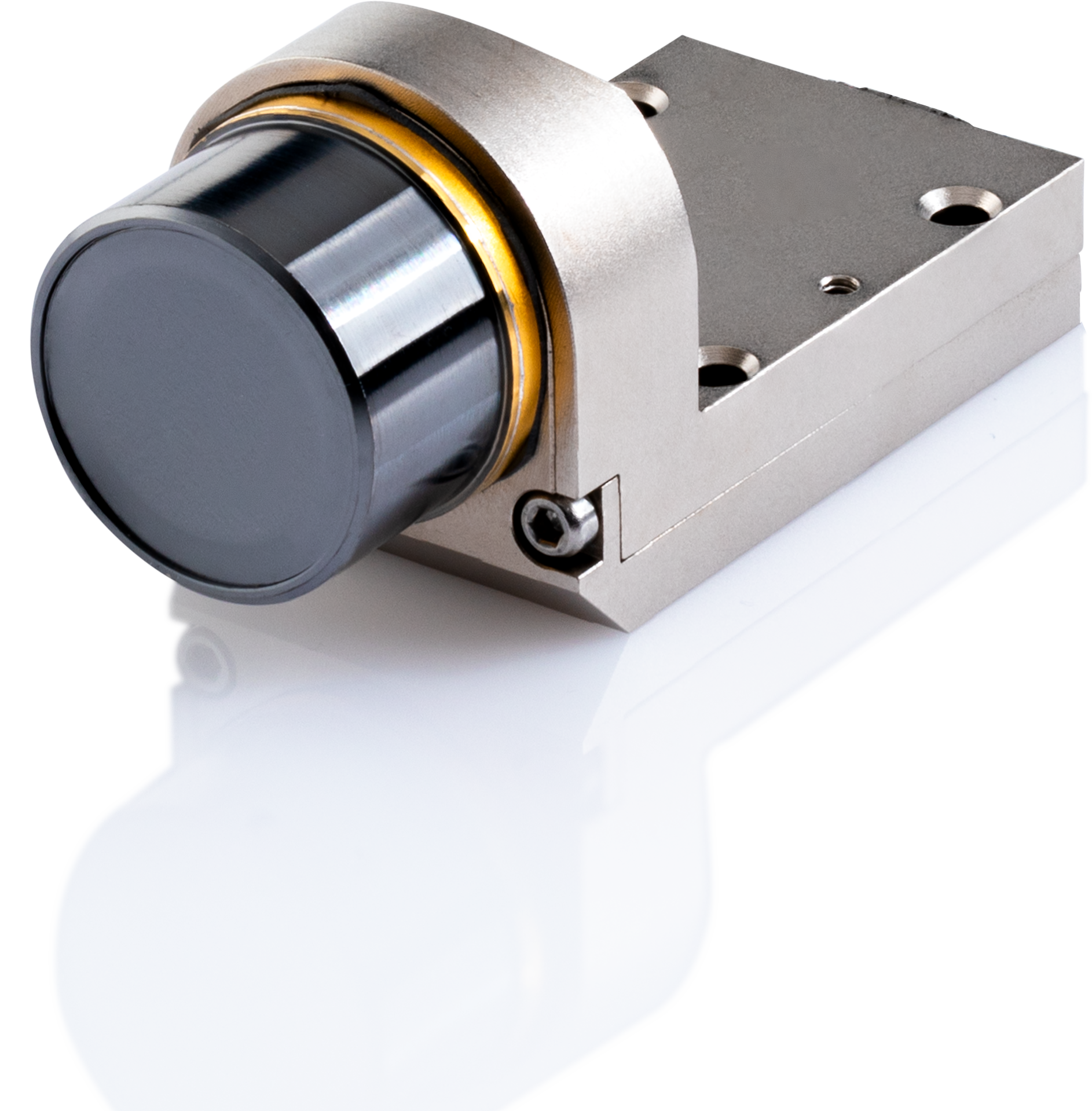
VIAMP KL 3.0 with a VITUS H150 BE

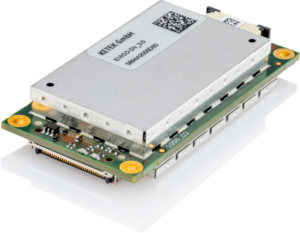
VIAMP KC 3.0 with VICO-DV 3.0 complete electronics board with DPP 3.0

VIAMP KC 3.0 with VICO-DV 3.0 complete electronics board with DPP 3.0, back view
Specifications
| First amplification stage | KETEK CSA |
| Energy resolution (@ Mn Kα, -45 °C chip temperature and 1 µs peaking time) | ≤ 136 eV |
| Peak to background | > 10,000 |
| Peak to tail | > 2,000 |
| Peak shift stability up to 100 kcps | < 1 eV |
| Max. input countrate | 1,000 kcps |
| Window | 25 µm Beryllium |
| Cooling performance at +20 °C heat sink temperature |
∆T > 80 K |
Spectrum
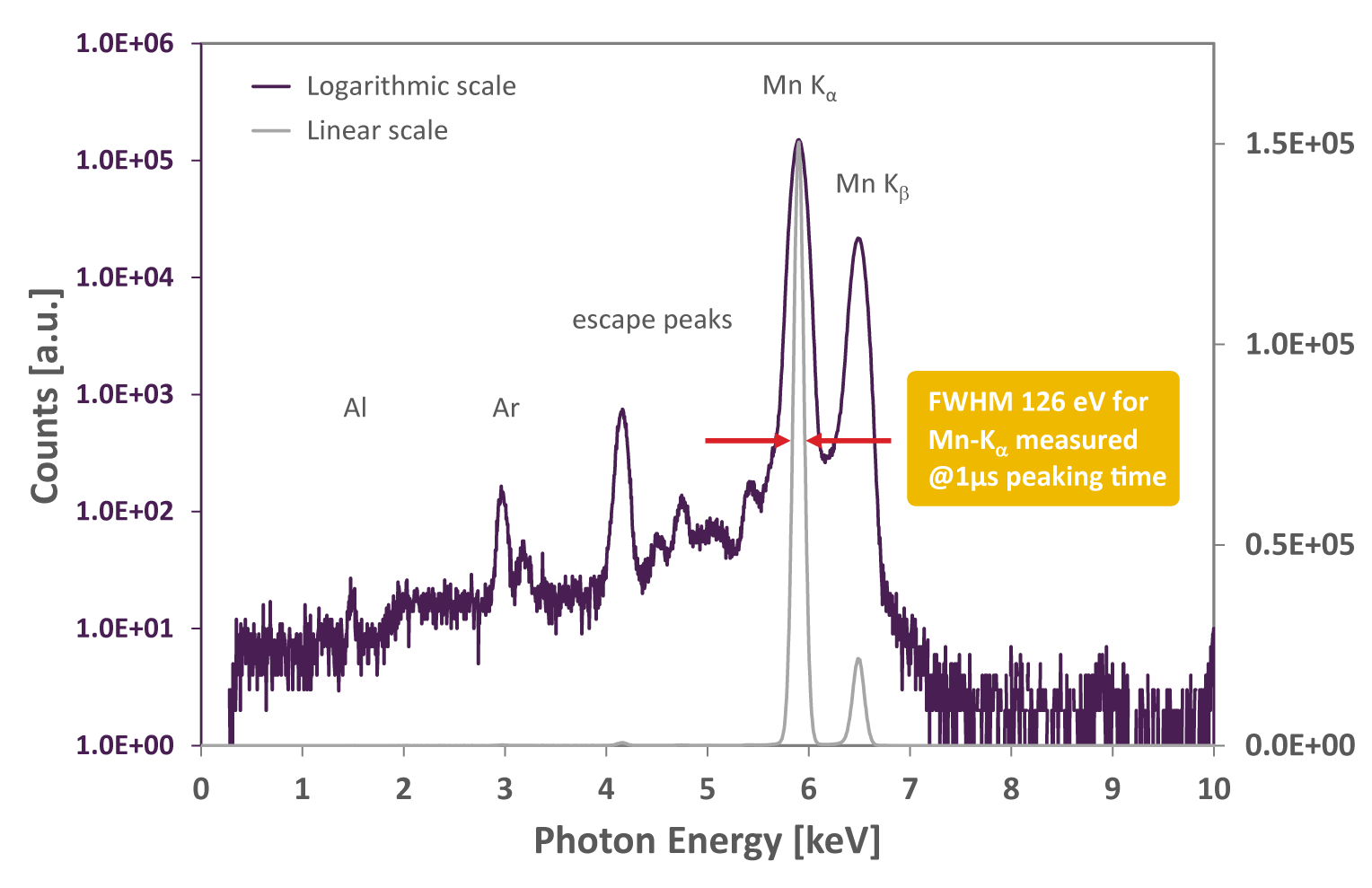
The spectrum of a VIAMP-KL 3.0 with a VITUS H150 SDD has been acquired in KETEK’s standard end qualification test stand. The input count rate has been 50 kcps at a peaking time of 1 μs and a SDD chip temperature of -45 °C. The spectrum shows an excellent peak-to-background ratio and energy resolution for Mn Kα.
Energy Resolution

This plot shows the energy resolution for Mn Kα measured with a VIAMP-KL 3.0 with a VITUS H150 SDD at different peaking times from 100 ns to 8 μs at a SDD chip temperature of -45 °C. The best set of parameters depend on the application optimizing either the energy resolution or the achievable through put.
Operating Parameters
| Parameter | Typical | Maximum Ratings |
| Positive Power Supply DC | +5 V 18 mA |
+4.9 V to +5.4 V 22 mA max |
| Negative Power Supply DC | -5 V 8 mA |
-5.4 V to -4.9 V 12 mA max |
| Output Signal | Positive Ramp | |
| Output Amplitude | ±0.975 V | ±0.95 Vpp,min ±1.0 Vpp,max |
| Output Gain* | 5 mV/keV | ±20 % |
| Gain Stability | < 20 ppm/°C | |
| External Reset (VICO-DV 3.0) | 0 V or + 3.3 V | |
| HV Supply DC | -168 V 125 µA |
±5 V 200 µA max |
| TEC Supply DC | 320 mA / 3.2 V @ -45 °C | 1000 mA / 9.2 V |
| TEC ΔT | > 80 K @ +20 °C heat sink temp. | |
| Temp. Sensor | 10 kΩ Thermistor @ +25 °C | ≤ 1 μA |
| * other gain on request |
Operation Block Diagram
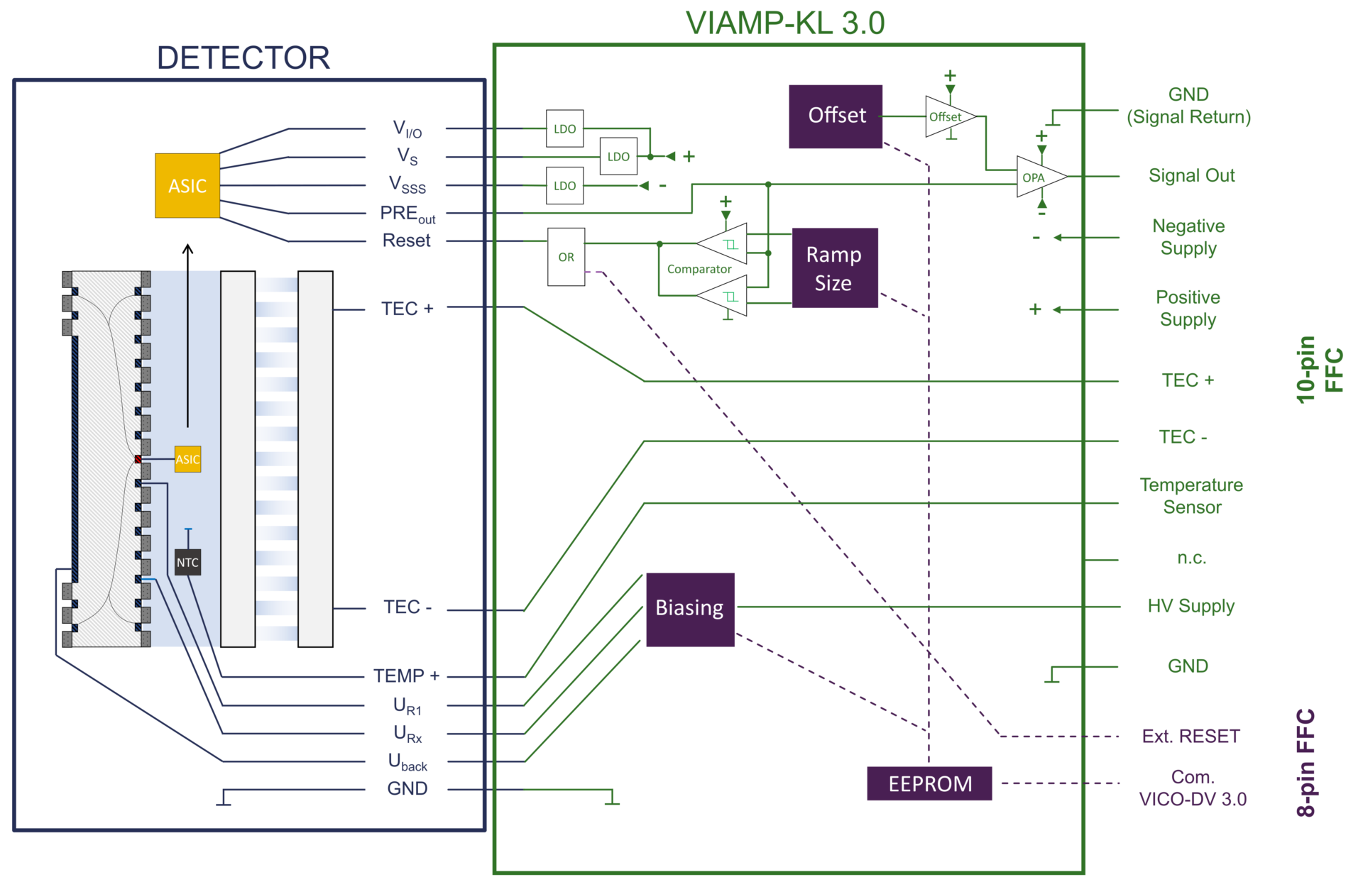
FFC connection

8-Pin FFC
VIAMP communication with VICO-DV 3.0 supply electronics
FFC Cable Length
The flat flexible cable is available in 50 mm, 100 mm and 200 mm length.
Pin Assignment 10-Pin FFC
| Pin 1 | TEC Return |
| Pin 2 | TEC Supply |
| Pin 3 | Positive Supply |
| Pin 4 | Negative Supply |
| Pin 5 | GND (Signal Return) |
| Pin 6 | Signal Out |
| Pin 7 | Temperature Sensor |
| Pin 8 | GND |
| Pin 9 | Not Connected |
| Pin 10 | HV Supply |
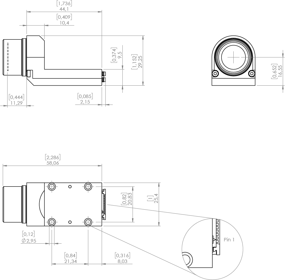
Geometry
Grounding and Thermal Scheme
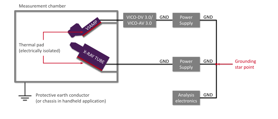
The VIAMP needs to be mounted using a gap pad which is electrically isolated but thermally conductive, as the VIAMP housing functions as heat sink.
Temperature Read-out
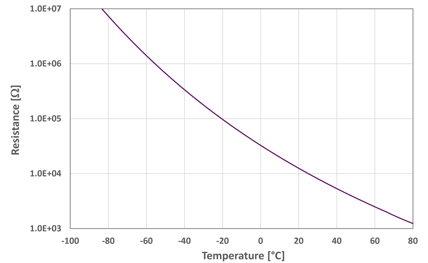
The temperature of the SDD chip is determined by a thermistor with a resistance-temperature correlation according to the following equation:

Related Products
Available Signal Processing Electronics & Accessories