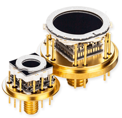
Microcell Construction
KETEK SiPM Technology
Technology with improved optical barrier and low-RC readout
Devices with low noise and improved timing
Best in class ratio of PDE vs. microcell size
Technology optimized for maximum fill factor
Devices with very high PDE
Different microcell sizes and active areas suitable for almost any application
KETEK Microcell Technology
KETEK Silicon Photomultipliers are based on a P-on-N structure: A shallow, highly P-doped region on top of a low N-doped common silicon body is forming the entrance window for the incoming light.
For this structure nearly all avalanche breakdowns are triggered by electrons. Due to the higher ionization coefficients for electrons the silicon, the P-on-N structure has a higher Geiger efficiency for blue- and UV light compared to a N-on-P structure. In addition, the dead layer of the PN-junction and the geometrical fill factor of the microcell have been continuously improved over the last years. Therefore KETEK is able to present Silicon Photomultipliers with highest PDE values for blue light.
The quenching resistor of a KETEK Silicon Photomultiplier is formed by a doped polysilicon strip line embedded in an insulating matrix. The resistivity can be precisely adjusted ensuring a high uniformity.
The entrance window of the light sensitive PN-junction is coated with an antireflective layer to avoid any reflection light losses at the interface.
In order to reduce the optical cross talk probability between individual microcells a very narrow vertical trench technology has been introduced. In addition, an effective impurity gettering has been implemented and the parasitic RC-values have been further reduced.