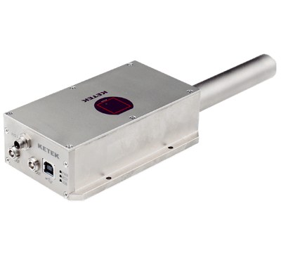
VITUS
H50
65 mm² collimated to 50 mm² X-ray Silicon Drift Detector for XRF – EDX – TXRF Applications
Unique Features
- 12.5 µm Be-Window
- High performance module
- Largest area in ultra compact TO8 housing
KEY PARAMETERS
(Guaranteed Values)
| CUBE CLASS |
|
|---|---|
| First amplification stage | ASIC |
| Energy resolution | ≤ 129 eV |
| Peak to background | > 15,000 |
| Peak to tail | > 2,000 |
| Optimal peaking time at max. cooling | 1 µs |
| Absorption depth | 450 µm Si |
| Peak shift stability up to 100 kcps | < 1 eV |
| Max. input countrate | 2,000 kcps |
| Windows | 12.5 µm Be |
| Cooling performance at +30°C heat sink temperature |
∆T > 75 K |
| On-chip collimator | multilayer |
| Ordering codes | V5C2T0-H50-ML9BEV 129 |
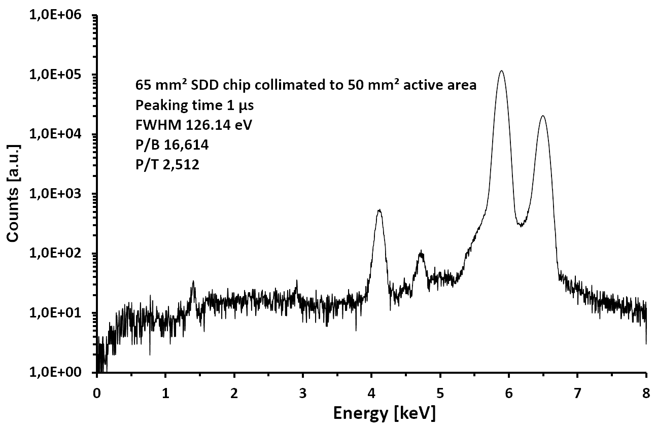
Spectrum
Figure 1: The spectrum has been acquired in KETEK’s standard end qualification test stand with an Fe-55 source using an XIA Mercury signal processing unit. The input count rate has been 10 kcps at a peaking time of 1 µs. The spectrum shows a very good energy resolution for Mn-Kα and an excellent peak-to-background ratio.
Energy Resolution
Figure 2: Energy resolution (Mn-Kα) values for peaking times from 0.1 µs through 8 µs showing good FWHM values even for higher operating temperatures. Depending on the application the best performance can be achieved by an appropriate selection of peaking time and set operating temperature.
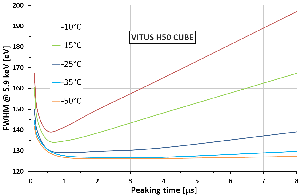
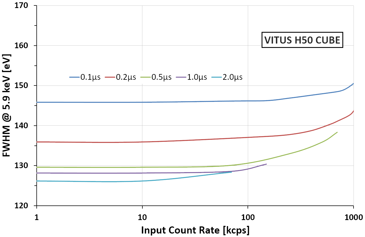
Figure 3: The VITUS H50 shows excellent energy resolution stability for different input count rates up to reasonable deadtimes at each peaking time. The data was measured at optimum cooling witKetek Vitus SDD H50 Energy Resolution vs. Input Count Rate for different Peaking Times an Fe-55 source using an XIA Mercury signal processing unit.
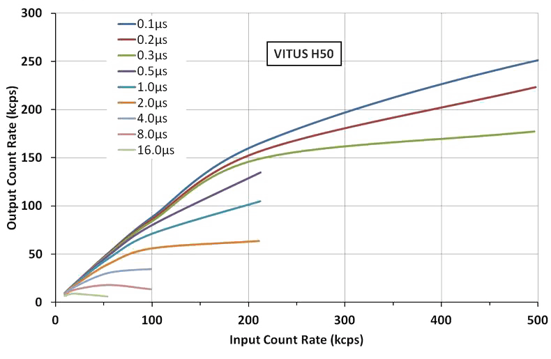
Throughput
Figure 4: The achievable VITUS H50 throughput is mainly influenced by the applied signal processing electronics. The shown data has been allocated with an XIA Mercury digital pulse processor which yields in an excellent throughput performance.
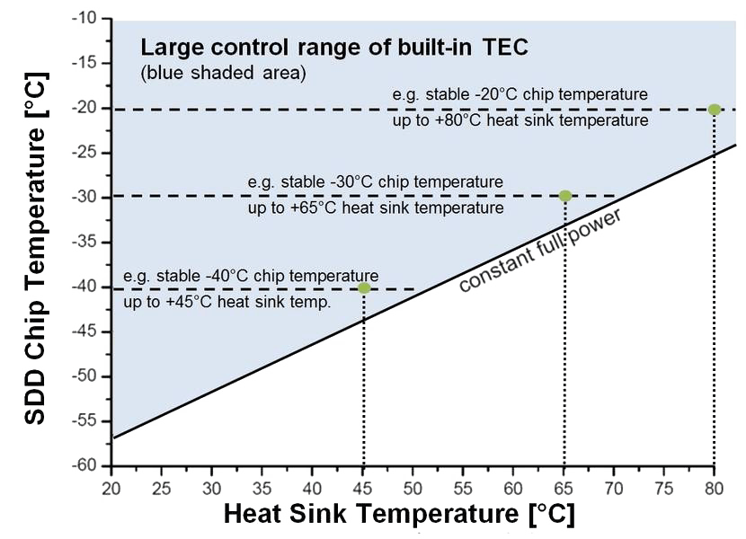
Control Range
Figure 5: The VITUS H50 can be operated at high ambient temperatures. The control range is given by the blue shaded area. Up to 80°C heat sink temperature the SDD can be operated stable at -20°C chip temperature without secondary cooling stage.
OPERATION REQUIREMENTS
SDD Voltages and Currents
| Ring1 (R1) | -20 V ± 5 V | 10 µA typ. |
|---|---|---|
| RingX (RX) | -130 V ± 20 V | 10 µA typ. |
| Back | -60 V ± 5 V | < 1 nA |
| Peltier Element | 3.6 V | 700 mA max. |
General parameters
| Temperature Monitor | NTC thermistor | 10 kΩ @ 25 °C |
|---|---|---|
| Output signal | ramped reset type | – |
CUBE based SDDs
| VI/O | 3.3 V ± 0.1 V | < 1 mA |
|---|---|---|
| Vs | 2 V ± 0.1 V | < 1 mA |
| Vsss | -5 V ± 0.1 V | < 1 mA |
| Output gain | 1.6 mV/keV ± 20 % | – |
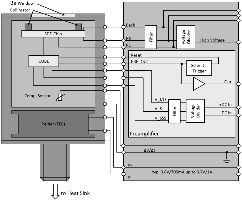
Operation
Block Diagram
Pin Assignment

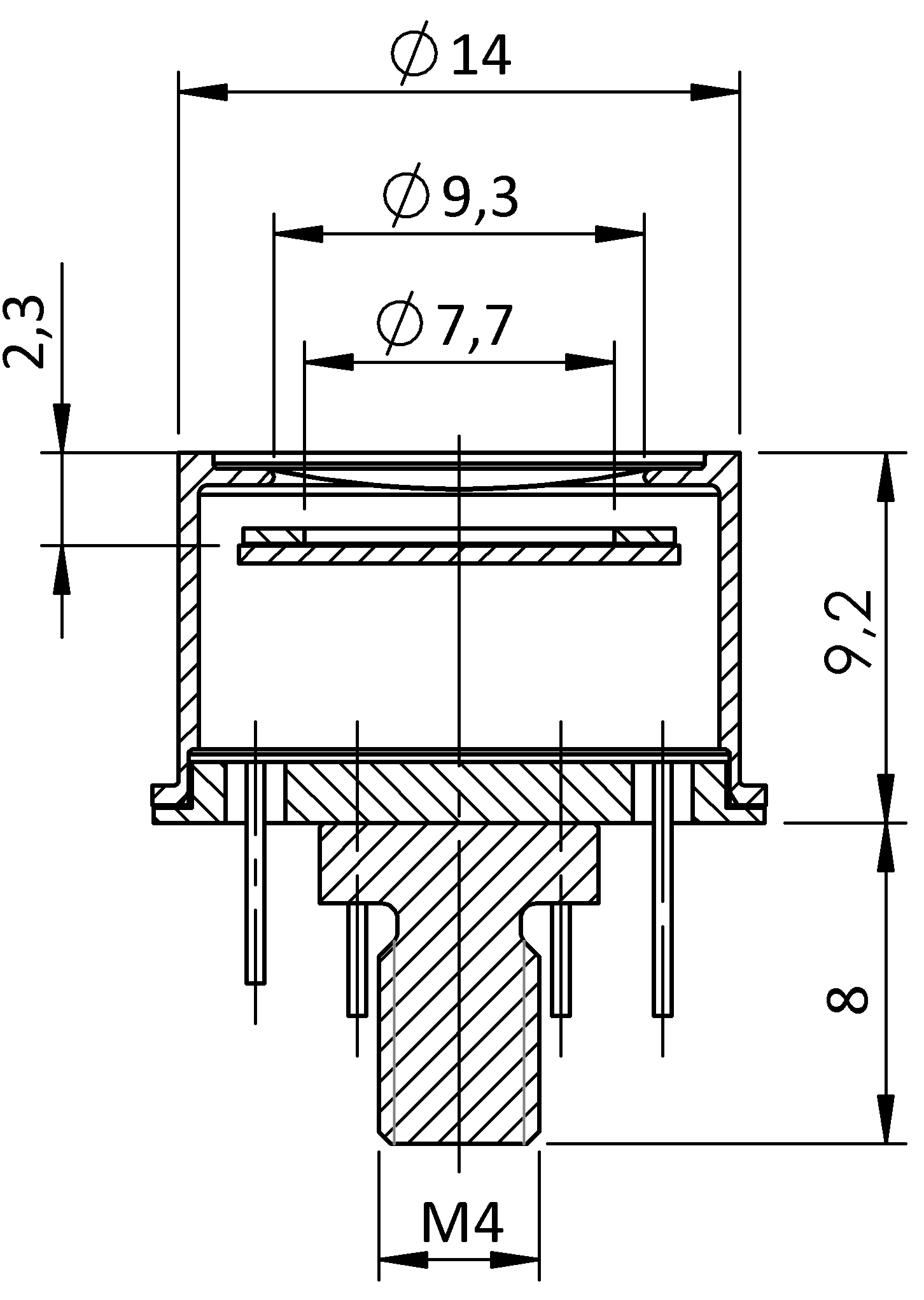
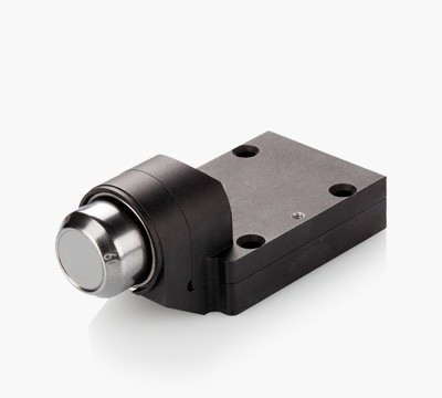
Geometry
Related Products
Available Signal Processing Electronics & Accessories
AXAS-A
Analytical X-ray Acquisition System – Analog
AXAS-D
Analytical X-ray Acquisition System – Digital
VIAMP
OEM solution with VITUS CUBE SDD and low-noise preamplifier

EMLCOL
External multilayer collimator to protect the SDD’s entrance window